9th - 12th July
1) Integrated clock aligner module with Simulation file.
2) Updated PRBS module to work with data_width = 20.
3) Updated prbs_control file to first align bits received from the RX interface.
4) Received FPGA sent by Florent.
Next Steps :
1) Implement design on FPGA.
2) Add functionality to read/ write primitive attributes using DRP interface.
We have discussed a rough plan for the coming month
Till 15th July - Integrate Clock aligner Module, implement on FPGA and debug if any issues. If time permits code functions to read/write primitive attributes using DRP interface
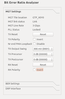
15th July - 23rd July - Add features: 1) RX/TX reset, channel reset 2) PLL Lock status 3) Link 4) Loopback mode 5) TX/RX Polarity
23rd July - 31st July - 1) TX Output Swing 2) Precursor control 3) Post cursor control
1st Aug - 6th Aug - Explore Eye scan architecture and if time permits, plot the same.
7th Aug - 12th Aug - Documentation, merging of code and submissions
2) Updated PRBS module to work with data_width = 20.
3) Updated prbs_control file to first align bits received from the RX interface.
4) Received FPGA sent by Florent.
Next Steps :
1) Implement design on FPGA.
2) Add functionality to read/ write primitive attributes using DRP interface.
We have discussed a rough plan for the coming month
Till 15th July - Integrate Clock aligner Module, implement on FPGA and debug if any issues. If time permits code functions to read/write primitive attributes using DRP interface
15th July - 23rd July - Add features: 1) RX/TX reset, channel reset 2) PLL Lock status 3) Link 4) Loopback mode 5) TX/RX Polarity
23rd July - 31st July - 1) TX Output Swing 2) Precursor control 3) Post cursor control
1st Aug - 6th Aug - Explore Eye scan architecture and if time permits, plot the same.
7th Aug - 12th Aug - Documentation, merging of code and submissions

Comments
Post a Comment